 |
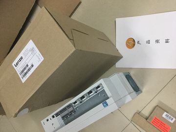
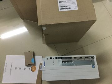
| Place of Origin: | GERMANY |
| Brand Name: | LENZE |
| Certification: | CE |
| Model Number: | E94ASSE0474 |
| Minimum Order Quantity: | 1pcs |
|---|---|
| Packaging Details: | carton |
| Delivery Time: | in stock |
| Payment Terms: | T/T, Western Union, MoneyGram |
| Supply Ability: | 100pcs/week |
| LENZE: | LENZE | E94ASSE0474: | E94ASSE0474 |
|---|---|---|---|
| GERMANY: | GERMANY | Temperature: | 20-90 |
| Color: | Black | Dimension: | 80mm |
| Wire: | Wire | Material: | Iron |
![]()
![]()
![]()
![]()
| resistance-type sensors or thermal resistors at the channel available for this (channel 4). |
Equotential bonding cable (optional) ⑥ 3-wire connection |
| 3-wire connection Note that line resistances are not compensated with a 3-wire connectionAnalog-to-digital |
Infeed element (for shielding only) ④ Digital-to-analog converter (DAC) |
| converter (ADC) ② LED interface |
Figure 4-7 Block diagram and terminal assignment for 3-wire connectionThe following figure shows the terminal assignment for 2-wire connection of resistance-type |
ensors or thermal resistors at the channel available for this (channel 4).
Note
2-wire connection
Note that line resistances are not compensated with a 2-wire connection.Analog-to-digital converter (ADC)
② LED interface
③ Infeed element (for shielding only)
④ Digital-to-analog converter (DAC)
⑤ Equotential bonding cable (optional)
⑥ 2-wire connection
Figure 4-8 Block diagram and terminal assignment for 2-wire connectionThe figure below shows the terminal assignment for the wiring of the voltage outputs with:
● 2-wire connection without compensation for line resistanceAnalog-to-digital converter (ADC)
② LED interface
③ Infeed element (for shielding only)
④ Digital-to-analog converter (DAC)
⑤ 2-wire connection CH0 and CH1
Figure 4-9 Block diagram and terminal assignment for voltage output
Note
MANA on terminals 19 and 20 is equivalent.nalog-to-digital converter (ADC)
② LED interface
③ Infeed element (for shielding only)
④ Digital-to-analog converter (DAC)
⑤ Current output CH0 and CH1
Figure 4-10 Block diagram and terminal assignment for current output
Note
MANA on terminals 19 and 20 is equivalent.This section contains the block diagram of the digital on-board I/O (X11) with standard inputs
and outputs and the encoder supply, as well as the rules for the correct wiring of the ground
connections.
For information on wiring the front connector, establishing the cable shield, etc., refer to the
, ET 200MPThe infeed element is inserted on the front connector and serves to shield the digital onboard
I/O.
Note
The digital on-board I/O is supplied via the front connector terminals and therefore does not
require power to be supplied by the infeed element. The infeed element is, however,
necessary for shieldingEncoder supply for the digital inputs
② CPU interface
xL+ Connection for 24 V DC supply voltage
xM Connection for ground
CHx Channel or channel status LED (green)
RUN Status display LED (green)
ERROR Error display LED (red)
PWR POWER supply voltage LED (green)
Figure 4-11 Block diagram and terminal assignment
NOTICE
Polarity reversal of the supply voltage
An internal protective circuit protects the digital on-board I/O against destruction if the
polarity of the supply voltage is reversed. In the case of polarity reversal of the supply
voltage, however, unexpected states can occur at the digital outputThe inputs and outputs of the digital on-board I/O are divided into two load groups which are
supplied with 24 V DC.
The digital inputs DI0 to DI15 form a load group and are supplied via the connections 1L+
(terminal 19) and 1M (terminal 20).
The digital outputs DQ0 to DQ7 are supplied via the connection 2L+ (terminal 29). The digital
outputs DQ8 to DQ15 are supplied via the connection 3L+ (terminal 39). Please note that the
digital outputs DQ0 to DQ15 only have a common ground. In each case, they are led through
to the two terminals 30 and 40 (2M/3M) and bridged in the module. The digital outputs form a
common load group.
Response of the digital outputs to a wire break at ground connection of the outputs
Due to the characteristics of the output driver used in the module, approx. 25 mA supply
current flows out through the outputs via a parasitic diode in the event of a ground wire
break. This behavior can lead to non-set outputs also carrying high levels and emitting up to
25 mA output current. Depending on the type of load, 25 mA can be sufficient to control the
load with high level. To prevent unintended switching of the digital outputs in the event of a
ground wire break, follow these steps:
Wire to ground twice
Connect ground to terminal 30 and to terminal 40.
1. Route the first ground connection from terminal 30 to the central ground connection of the
plant.
2. Route the second ground connection from terminal 40 to the central ground connection of
the plant.
If terminal 30 or 40 are interrupted by a ground wire break, the outputs will continue to be
supplied via the second, intact ground connection.
WARNING
Wire break at ground connection
Never bridge from terminal 30 to terminal 40 in the front connector and never lead only one
wire to the central ground connection.
Connect terminal 30 and terminal 40 to a common ground pointThe ground is supplied with a first cable from the central terminal block to terminal 30 of the