 |
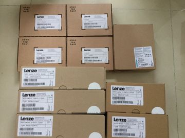
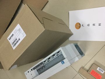
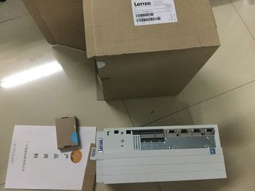
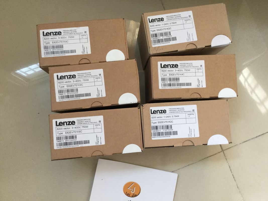
| Place of Origin: | GERMANY |
| Brand Name: | LENZE |
| Certification: | CE |
| Model Number: | E94ASSE0864 |
| Minimum Order Quantity: | 1pcs |
|---|---|
| Packaging Details: | carton |
| Delivery Time: | in stock |
| Payment Terms: | T/T, Western Union, MoneyGram |
| Supply Ability: | 100pcs/week |
| LENZE: | LENZE | GERMANY: | GERMANY |
|---|---|---|---|
| MATERIAL: | IRON | COLOR: | BLACK |
| Temperature: | 20-90 | Dimension: | 80mm |
| Wire: | Wire | E94ASSE0864: | E94ASSE0864 |
![]()
![]()
![]()
![]()
| The encoder or sensor switches the A, B and N inputs to 24 V DC. Note |
|
| External load resistance Note that, depending on the characteristics of the signal source, effective load and height |
|
| of the signal frequency, you may require an external load resistance to limit the fall time of the signal from high level to low level. |
The specifications/technical data of the signal source (e.g. sensor) are decisive for the
configuration of such a load resistance.
● Push-pull:
The encoder or sensor switches the A, B and N inputs alternately to 24 V DC and to The digital inputs are logically assigned to the high-speed counters (HSC). For information
on the possible assignment of the on-board I/O inputs to the high-speed counters, refer to
the table Interconnection overview of the inputs (Page 98). Up to two digital inputs are
available for each high-speed counter (HSC DI0 and HSC DI1). You can use the digital
inputs for the gate control (Gate), synchronization (Sync) and Capture functions.
Alternatively, you can use one or more digital inputs as standard digital inputs without the
functions mentioned and read the signal state of the respective digital input using the
feedback interface.
Digital inputs that you do not use for high-speed counting are available for use as standard
DIs.You set the digital input addresses used by the high-speed counters (HSC) and the
assignment of A/B/N, DI0, DI1 and DQ1 signals in STEP 7 (TIA Portal). You can enable and
configure each HSC when you configure the compact CPU.
The compact CPU assigns the input addresses for the A/B/N signals automatically according
to the configuration.
You specify the input addresses for DI0 and DI1 according to the table Interconnection
overview of the inputs (Page 98). The interconnection produces a direct connection of the
HSC to an input of the on-board I/O. The high-speed counter then uses this input as HSC
DI0 or HSC DI1 ([DI] symbol). The [DI] symbols in the table identify the input addresses for
HSC DI0 and HSC DI1 that are offered for selection in the hardware configuration.
Assignment of HSC addresses of inputs
You can find an overview of the options for interconnecting the inputs of the front connectors
X11 and X12 in the section Interconnection overview of the inputs (Page 98).
Digital outputs HSC-DQ0 and HSC-DQ1
Two digital outputs are available for each high-speed counter. Digital output HSC-DQ0 is a
logical output that cannot be interconnected with a digital output of the on-board I/O. Digital
output HSC-DQ0 can only be used via the user program. HSC-DQ1 is a physical output that
can be interconnected with a digital output of the on-board I/O.
The digital outputs are 24 V sourcing output switches relative to M and can be loaded with a
rated load current of 0.1 A. The outputs used as standard outputs have a rated load current
of 0.5 A. The digital outputs are protected against overload and short-circuit.
Note
It is possible to directly connect relays and contactors without external wiring. For information
on the maximum possible operating frequencies and the inductance values of the inductive
loads at the digital outputs, refer to the Technical specifications section.
The section Interconnection overview of the outputs (Page 99) provides an overview of
which digital outputs you can interconnect to which high-speed counters. Digital outputs to
which no high-speed counter is interconnected can be used as standard outputs. The
maximum output delay of each digital output used as standard output is 500 μs.You assign the digital inputs and outputs to the pulse duration modulation (PWM) and the
pulse train output (PTO) during the device configuration. If you assign digital inputs and
outputs to these functions, the values of the addresses of the assigned digital inputs and
outputs cannot be changed by the function for forcing in the watch table. Instead, you can
force the output bit TM_CTRL_DQ to 0 and switch the output on or off with the bit SET_DQA
(relevant for the PWM and Frequency Output modes).
For more information on forcing inputs and outputs, refer to the , ET 200MP system In addition to supporting its outputs, each PTO channel also supports the three following
optional inputs:
● Reference Switch (RS)
● Measuring Input (MI)
● Drive Ready (DR)
Input addresses of the pulse generators (PTO)
You make the settings of the digital input addresses used by the pulse generators (PTO) in
the hardware configuration of STEP 7 (TIA Portal). When you configure the compact CPU,
you can individually activate and configure the four PTO channels.
Assignment of PTO addresses of inputs
A direct connection from the PTO to an input of the on-board I/O is established through the
interconnection. You can find an overview of the options for interconnecting the inputs (DI0
to DI15) to the available PTO channels (PTO1 to PTO4) in the section Interconnection
overview of the inputs (Page 98)You connect the encoder signals, the digital input and output signals and the encoder supply
to the 40-pin front connector of the digital on-board I/O. For information on wiring the front
connectors, establishing the cable shields, etc., refer to the , ET 200MP system
manual.The following table provides you with an overview of the possible interconnections of the
inputs of front connector X11 to allow you to correctly distribute the available inputs over the
possible technology channels HSC and PTO. This overview is a combination of
interconnection options of technology channels for HSC and PTO.The following table provides you with an overview of the possible interconnections of the