 |
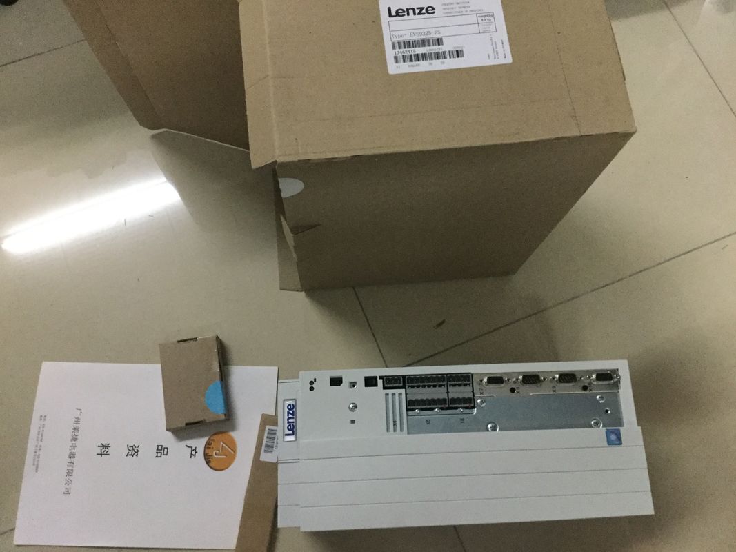
| Place of Origin: | GERMANY |
| Brand Name: | LENZE |
| Certification: | CE |
| Model Number: | EVS9329-EI |
| Minimum Order Quantity: | 1pcs |
|---|---|
| Packaging Details: | carton |
| Delivery Time: | in stock |
| Payment Terms: | T/T, Western Union, MoneyGram |
| Supply Ability: | 100pcs/week |
| LENZE: | LENZE | EVS9329-EI: | EVS9329-EI |
|---|---|---|---|
| GERMANY: | GERMANY | Temperature: | 20-90 |
| Wire: | Wire | Color: | Black |
| Dimension: | 80mm |
| or the neighborhood discovery function. The number range of the MAC addresses is continuous. The first and last MAC address are |
|
| lasered on the rating plate on the right side of each CPU 1512C-1 PN. The table below shows how the MAC addresses are assigned. |
|
| Table 4- 1 Assignment of the MAC addresses |
Two digital outputs are available for each high-speed counter. Digital output HSC-DQ0 is a
logical output that cannot be interconnected with a digital output of the on-board I/O. Digital
output HSC-DQ0 can only be used via the user program. HSC-DQ1 is a physical output that
can be interconnected with a digital output of the on-board I/O.
The digital outputs are 24 V sourcing output switches relative to M and can be loaded with a
rated load current of 0.1 A. The outputs used as standard outputs have a rated load current
of 0.5 A. The digital outputs are protected against overload and short-circuit.
Note
It is possible to directly connect relays and contactors without external wiring. For information
on the maximum possible operating frequencies and the inductance values of the inductive
loads at the digital outputs, refer to the Technical specifications section.
The section Interconnection overview of outputs (Page 111) provides an overview of which
digital outputs you can interconnect to which high-speed counters. Digital outputs to which
no high-speed counter is interconnected can be used as standard outputs. The maximum
output delay of each digital output used as standard output is 500 µs.
Shielding
Note
When you use digital inputs/outputs with technology functions, i.e. interconnect high-speed
counters with the inputs/outputs, you must use shielded cables and the infeed element for
shielding.When you use digital inputs/outputs with technology functions, i.e. interconnect high-speed
counters with the inputs/outputs, you must use shielded cables and the infeed element for
shielding.
Reference
For more information on configuring the inputs of the high-speed counters, refer to the
, ET 200MP, ET 200SP Counting, measurement and position detection If you configure the memory of the outputs of the CPU as pulse generators (for PWM or
PTO), the corresponding addresses of the outputs are removed from the memory. You
cannot use the addresses of the outputs for other purposes in your user program. When your
user program writes a value to an output that you are using as a pulse generator, the CPU
does not write this value to the physical output.
Assignment of the PWM addresses of the outputs
The section Interconnection overview of outputs (Page 111) provides an overview of which
digital outputs you can interconnect to which PWM channels.
Note
The digital inputs and outputs assigned to PWM and PTO cannot be forced.
You assign the digital inputs and outputs to the pulse duration modulation (PWM) and the
pulse train output (PTO) during the device configuration. If you assign digital inputs and
outputs to these functions, the values of the addresses of the assigned digital inputs and
outputs cannot be changed by the function for forcing in the watch table. Instead, you can
force the output bit TM_CTRL_DQ to 0 and switch the output on or off with the bit SET_DQA
(relevant for the PWM and Frequency Output modes).
For more information on forcing inputs and outputs, refer to the , ET 200MP system You connect the encoder signals, the digital input and output signals and the encoder
supplies to the two 40-pin front connectors of the digital on-board I/O. For information on
wiring the front connectors and establishing the cable shield, refer to the , ET In addition to supporting its outputs, each PTO channel also supports the three following
optional inputs:
● Reference Switch (RS)
● Measuring Input (MI)
● Drive Ready (DR)
Input addresses of the pulse generators (PTO)
You make the settings of the digital input addresses used by the pulse generators (PTO) in
the hardware configuration of STEP 7 (TIA Portal). When you configure the compact CPU
you can individually activate and configure the four PTO channels.
Assignment of PTO addresses of inputs
A direct connection from the PTO to an input of the on-board I/O is established through the
interconnection. You can find an overview of the options for interconnecting the inputs (DI0
to DI15) to the available PTO channels (PTO1 to PTO4) in the section Interconnection
overview of the inputs (Page 109).The section Interconnection overview of outputs (Page 111) provides an overview of which
digital outputs you can interconnect to which PTO channels.In order that you can correctly divide the available inputs between the possible technology
channels HSC and PTO, the following table provides you with an overview of the possible
interconnections of the front connectors X11 and X12. This overview] = Drive Ready; [MI] = Measuring Input; [RS] = Reference Switch
[DI] stands for [HSC DI0/HSC DI1] = DI: Is used for the HSC functions: Gate, Sync and Capture
The assignment to [B] or [N] takes precedence over the assignment to HSC DI0 or HSC DI1. This means that input addresses
that are assigned to count signal [B] or [N] based on the selected signal type cannot be used for other signals
such as HSC DI0 or HSC DI1.The following table provides you with an overview of the possible interconnections of the
front connectors X11 and X12 to allow you to correctly divide the available inputs between
the possible technology channels HSC, PWM and PTO. This overview is a combination of
interconnection options of technology channels for HSC, PWM and PTO) With sourcing outputs, it must be taken into consideration that falling edges can be delayed as compared to rising edges
depending on the load. The on-load factor can therefore be falsified. Consider using a high-speed output if the load at
the output is greater than 240 Ω.
2) The frequency has a basic accuracy of ±100 ppm with a resolution of 0.3638 mHz.
3) Standard outputs are affected by jitter during generation of frequencies. The set period duration is not adhered to in
every period, but it is adhered to on average over several periods.The addresses are divided into five analog input channels and two analog output channels.
STEP 7 (TIA Portal) assigns the addresses automatically. You can change the addresses in
the hardware configuration of STEP 7 (TIA Portal), i.e. freely assign the start address. The
addresses of the channels are based on the start address.
"IB x" stands, for example, for the start address input byte x. "QB x" stands, for example, for
the start address output byte xThe value status = 1 ("Good") indicates that the process value specified by the user program
is correctly output at the terminal.
The value status = 0 ("Bad") indicates that the process value output at the hardware output is
incorrect.
Possible cause for value status = 0:
● a channel has been deactivated
● Outputs are inactive (for example, CPU in STOP)
● An output value is outside the lower/upper measuring range (overflow/underflow)
● Wire break has occurred (only for the "Current" output type)
● Short-circuit has occurred (only for the "Voltage" output typeT