 |
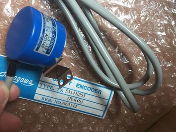
| Place of Origin: | Japan |
| Brand Name: | Tamagawa |
| Certification: | CE |
| Model Number: | TS5016N63 |
| Minimum Order Quantity: | 1pcs |
|---|---|
| Packaging Details: | carton |
| Delivery Time: | in stock |
| Payment Terms: | T/T, Western Union, MoneyGram |
| Supply Ability: | 100pcs/week |
| Tamagawa: | Tamagawa | TS5016N63: | TS5016N63 |
|---|---|---|---|
| Japan: | Japan | Material: | Iron |
| Color: | Black | Temperature: | 30-80 |
| WIRE: | Wire |
| assignment (= and /=) boxes where you specify a bit | You can specify an immediate write of a physical output using ":P" following the Q offset (example: "%Q3.4:P"). |
| address for the box output. Box inputs and outputs can be | For an immediate write, the bit data values are written to the process image output and directly to physical output. |
| connected to other box logic or you can enter a bit address. |
output coil or an FBD "=" box is enabled, then the output |
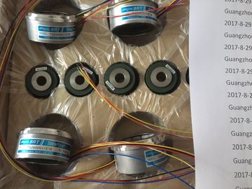
Guang Zhou Lai Jie Electric Co.,LTD
TS5016N63
TS3630N3E6
TS3630N1303E9
TS3630N1306
TS3630N11E1
TS3630N11E2
TS3630N12E3
TS3630N12E4
TS3630N13E5
TS3630N13E6
FA-CODER
TS5214N566
TS5205N450
TS5205N454
TS5205
N450
TS5205
N454
TS5205N452
TS5205
N452
TS5207
TS5208
If there is no power flow through an output coil or an FBD "=" assignment box is not
enabled, then the output bit is set to 0.
● If there is power flow through an inverted output coil or an FBD "/=" box is enabled, then
the output bit is set to 0.
● If there is no power flow through an inverted output coil or an FBD "/=" box is not enabled,
then the output bit is set to 1. When S (Set) is activated, then the data value at the OUT
address is set to 1. When S is not activated, OUT is not
changed.
Not available When R (Reset) is activated, then the data value at the OUT
address is set to 0. When R is not activated, OUT is not
changed. IN (or connect to contact/gate logic) Bool Bit location to be monitored
OUT Bool Bit location to be set or reset When SET_BF is activated, a data value of 1 is assigned to "n"
bits starting at address OUT. When SET_BF is not activated,
OUT is not changed.
Not available RESET_BF writes a data value of 0 to "n" bits starting at
address OUT. When RESET_BF is not activated, OUT is not
changed. Starting element of a bit field to be set or reset (Example:
#MyArray[3])
n Constant (UInt) Number of bits to write RS is a set dominant latch where the set dominates. If the set (S1) and reset (R)
signals are both true, the output address OUT will be 1.
Not available SR is a reset dominant latch where the reset dominates. If the set (S) and reset
(R1) signals are both true, the output address OUT will be 0. The OUT parameter specifies the bit address that is set or reset. The optional OUT output Q
reflects the signal state of the "OUT" address. LAD: The state of this contact is TRUE when a positive transition (OFFto-ON)
is detected on the assigned "IN" bit. The contact logic state is
then combined with the power flow in state to set the power flow out
state. The P contact can be located anywhere in the network except the
end of a branch.
FBD: The output logic state is TRUE when a positive transition (OFFto-ON)
is detected on the assigned input bit. The P box can only be
located at the beginning of a branch.
Not available LAD: The state of this contact is TRUE when a negative transition (ONto-OFF)
is detected on the assigned input bit. The contact logic state is
then combined with the power flow in state to set the power flow out
state. The N contact can be located anywhere in the network except
the end of a branch.
FBD: The output logic state is TRUE when a negative transition (ON-toOFF)
is detected on the assigned input bit. The N box can only be
located at the beginning of a branch. LAD: The assigned bit "OUT" is TRUE when a positive transition (OFFto-ON)
is detected on the power flow entering the coil. The power flow
in state always passes through the coil as the power flow out state. The
P coil can be located anywhere in the network.
FBD: The assigned bit "OUT" is TRUE when a positive transition (OFFto-ON)
is detected on the logic state at the box input connection or on
the input bit assignment if the box is located at the start of a branch.
The input logic state always passes through the box as the output logic
state. The P= box can be located anywhere in the branch.
Not available LAD: The assigned bit "OUT" is TRUE when a negative transition (ONto-OFF)
is detected on the power flow entering the coil. The power flow
in state always passes through the coil as the power flow out state. The
N coil can be located anywhere in the network.
FBD: The assigned bit "OUT" is TRUE when a negative transition (ONto-OFF)
is detected on the logic state at the box input connection or on
the input bit assignment if the box is located at the start of a branch.
The input logic state always passes through the box as the output logic
state. The N= box can be located anywhere in the branch. The Q output power flow or logic state is TRUE when a positive transition
(OFF-to-ON) is detected on the CLK input state (FBD) or CLK power flow
in (LAD).
In LAD, the P_TRIG instruction cannot be located at the beginning or end
of a network. In FBD, the P_TRIG instruction can be located anywhere
except the end of a branch.
Not available The Q output power flow or logic state is TRUE when a negative transition
(ON-to-OFF) is detected on the CLK input state (FBD) or CLK power flow
in (LAD).
In LAD, the N_TRIG instruction cannot be located at the beginning or end
of a network. In FBD, the N_TRIG instruction can be located anywhere
except the end of a branch. Memory bit in which the previous state of the input is saved
IN Bool Input bit whose transition edge is to be detected
OUT Bool Output bit which indicates a transition edge was detected
CLK Bool Power flow or input bit whose transition edge is to be detected
Q Bool Output which indicates an edge was detected All edge instructions use a memory bit (M_BIT) to store the previous state of the input signal
being monitored. An edge is detected by comparing the state of the input with the state of
the memory bit. If the states indicate a change of the input in the direction of interest, then an
edge is reported by writing the output TRUE. Otherwise, the output is written FALSE.
Note
Edge instructions evaluate the input and memory-bit values each time they are executed,
including the first execution. You must account for the initial states of the input and memory
bit in your program design either to allow or to avoid edge detection on the first scan.
Because the memory bit must be maintained from one execution to the next, you should use
a unique bit for each edge instruction, and you should not use this bit any other place in your
program. You should also avoid temporary memory and memory that can be affected by
other system functions, such as an I/O update. Use only M, global DB, or Static memory (in
an instance DB) for M_BIT memory assignments.
7.2 Timers
You use the timer instructions to create programmed time delays. The number of timers that
you can use in your user program is limited only by the amount of memory in the CPU. Each
timer uses a 16 byte IEC_Timer data type DB structure to store timer data that is specified at
the top of the box or coil instruction. STEP 7 automatically creates the DB when you insert
the instruction.The TONR timer sets output Q to ON after a
preset time delay. Elapsed time is accumulated