|
| Place of Origin: | Japan |
| Brand Name: | Tamagawa |
| Certification: | CE |
| Model Number: | TS5320N510 |
| Minimum Order Quantity: | 1pcs |
|---|---|
| Packaging Details: | carton |
| Delivery Time: | in stock |
| Payment Terms: | T/T, Western Union, MoneyGram |
| Supply Ability: | 100pcs/week |
| TAMAGAWA: | TAMAGAWA | Material: | Iron |
|---|---|---|---|
| Japan: | Japan | Color: | Black |
| Temperature: | 20-90 | Dimension: | 90mm |
| Wire: | Wire | TS5320N510: | TS5320N510 |
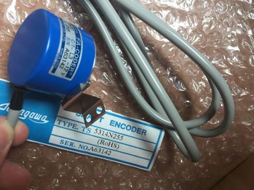
TS5320N510
| deactivated, faulty or inaccessible. |
information on addressing and address allocation with value status can be found in the manuals of the digital modules, and in the online help for STEP 7. An example of the |
| ou can find additional information on evaluation and processing of the value status for failsafe | evaluation of the value status in the user program is available in the function manual |
| igital modules in the SIMATIC Safety – Configuring and ProgrammingAdditional | DiagnosticsThe address of an analog channel is always a word address. The channel address depends |
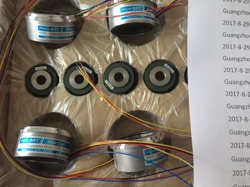
Guang Zhou Lai Jie Electric Co.,LTD
Please contact with “Tommy” for the price
TS4502N1000E200
TS4502N1202E200
TS4502N2000E100
TS4503N1000E200
TS4503N1007E200
TS4503N1022E100
TS4503N1022E200
TS4503N1202E200
TS4503N1205E200
TS4503N1828E100
TS4503N2000E100
TS4503N2070E100
TS4503N2202E200
TS4503N2036E501
TS4506N1202E200
TS4507N1002E200
TS4507N1202E200
TS4507N1205E200
TS4507N1229E200
TS4507N2000E100
TS4507N2070E100
TS4507N2405E200
TS4507N6205E200
TS4507N8029E200
TS4509N1002E200
TS4509N1202E200
TS4509N1831E200
TS4509N2002E200
TS4509N2405E200
TS4509N7000E100
TS4514N1021E200
TS4514N1407E200
TS4514N1828E200
TS4514N2002E200
TS4514N2405E200
TS4515N1202E200
TS4515N2405E200
on the module start address. STEP 7 automatically assigns the channel addresses during
configuration. Based on the module start addresses, STEP 7 assigns the channel addresses
in increasing sequence (in the following figure, the module start address is 256).
When you insert an analog module into a free slot, STEP 7 assigns a default address. You
can change the assigned default address in STEP 7.The following section describes the addressing of the analog modules. In your user program,
you require the addresses of the channels of the analog module.The following figure shows how the addresses of the individual channels of the analog input
module (e.g., 6ES7531-7NF10-0AB0) are determined when the module has the start
address 256.The value status is additional binary information of an analog input or output value. It is
entered simultaneously with the process value in the process image input and provides
information about the validity of the analog value.
If you enable the value status for an analog module, then additional bytes are allocated in
the input address area. Each bit in the value status is assigned to a channel and provides
information about the validity of the process value. You can find the assignment in the
product manual for the respective I/O module.
The value status is influenced by all diagnostics that might falsify the process value, e.g. wire
break, short-circuit.
● 1B: A valid process value is being output or read for the channel.
● 0B: A substitute value is being output for the channel, or the channel is deactivated, faulty
or inaccessibleAdditional information on addressing and address allocation with value status can be found
in the manuals of the analog modules, and in the online help for STEP 7. A detailed
description of the value status for analog modules is available in the function manual Analog
value processing (The process image of the inputs and outputs is an image of the signal states. The CPU
transfers the values from the input and output modules to the process image in this memory
area. At the start of the cyclic program, the CPU transfers the signal states of the input
modules to the process image input. At the end of the cyclic program, the CPU transfers the
process image output as a signal state to the output modules.
A process image allows you to access a consistent image of process signals during cyclic
program execution. If a signal state at an input module changes during program processing,
the signal state is retained in the process image. The CPU does not update the process
image until the next cycle.When the process image is updated, the accesses the data of each submodule as
consistent data. The maximum data width that is accessed as consistent data for